Control System for Multiband Microwave Station
Introduction
Over the
past few years I have been using PIC microcontrollers in a number of projects.
This started with a 2m transverter and control unit
which drives transverters for 13, 6 and 3cm, and continued
with my 23cm SSPA. This latest project extends that a bit further, using a more
modern PIC device.
The new
control box is intended to allow both of my HF prime mover rigs to be used with
a range of transverters. My Elecraft
K3 has been dedicated to 1.3GHz operation up to now, but it has many advantages
over the Elecraft K2 used for the high band transverters, so it makes sense to link it to a wider range
of kit. Retaining the K2 allows a degree of SO2R (Single Op 2 Radio) operation
in major contests, but it does mean that the control box has to resolve
conflicts between the
At the same
time I have taken the opportunity to support some future changes to the
station. I plan to replace my aging FT736R (used on 432MHz and transverting from there to 3400MHz) and existing 250W valve
PA with a new transverter from 28MHz and a new SSPA,
so the control box is designed to support this arrangement. I also plan to
change the dish feeds for 2.3 and 3.4GHz to concentric loop feeds, but this
means that isolation between the feeds will be quite low so an interlock is
needed to stop transmit power getting into the receiver front end for the other
band.
I have also
added a “transverter enable” feature which allows
unused transverters to be powered down, or the LO
injection disabled. This will reduce some IF breakthrough problems from the
local GB3MH* beacons, and make it easier to listen for weak beacons.
A couple of
future additions are catered for, one is a socket for a second K3 if I should
ever get round to replacing the
Design
Control Inputs
All of the
switchbox operation is controlled by the
The control
inputs are taken from parallel interfaces on the
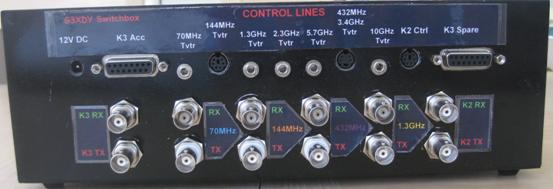
RF Switching
The switch
box is based on two switching matrices, one for receive and one for transmit.
Each can connect either of two inputs to four outputs. These matrices are used
to switch the low level 28MHz IF signals to and from the K2 and K3 to transverters for 70MHz, 144MHz (and 2.3, 5.7,10GHz), 432MHz
(and 3.4GHz) and 1.3GHz. The relays used (NAIS TQ2 range) are relatively cheap
but have reasonable RF performance at 28MHz, and are configured to maximise
isolation in the off state. Measurements made indicate that the minimum
isolation is 65dB, and through loss is negligible (<0.1 dB). Each switch
matrix board is controlled by a serial interface driver chip,
the two boards are cascaded and driven by three lines from the main control
processor (clock, data, and latch signals). The switch arrangement does allow
both receivers to be connected to one transverter if
required.
Control Lines
To provide
the transverter enable function I have used stereo
3.5mm jacks for most of the interfaces, with conventional “ground to transmit”
on the tip of the jack, and “ground to enable” on the ring contact. This means
that mono 3.5mm jacks can be used to operate transverters
with no enable features, but there is an easy upgrade path as I add this
capability to each band. The software support for transverter
enable is included in the initial build.
One exception
to the rule is 144MHz where the transverter control
also carries band select outputs to select higher band transverters
– this allows the existing transverter and switch box
to be used without modification. The other is the control connector for the
future 432MHz transverter which will also support the
3.4GHz transverter, so again a band select line is
also required.
All of the
control lines are driven by darlington
relay driver interface chips which provide a robust interface to the outside
world, they can sink currents of up to 500mA and withstand voltages to 50V. The
only downside is that the on state voltage drop is fairly high (about 1.2V)
which needs to be borne in mind with some interfaces.
LED indicators
LEDs are
used to indicate what band is in use for each rig, and whether on transmit of
receive. An LCD digital display might be simpler, but the LED status display is
easy to take in at a glance. The LED for a selected band will be Green on
receive and Red on transmit, all other LEDs for that
prime mover will be off. Any clash for resources will result in one rig
“winning” (generally the K3) and the LED for the other rig will display Amber
(by rapidly switching between Green and Red). The only exception to the K3
winning any contention is the interlock when the
Processor
The heart
of the control box is a PIC16F884 midrange PIC microcontroller. Even though
this has 36 I/O pins this is not sufficient for this application, so the
outputs are expanded in various ways, the serial interface to the switch matrix
relay driver being one example. For the control interface outputs two octal
latches expand Port C to give 16 lines. The LEDs are
driven from BCD decoders on two further latches on Port C. The BCD decoders
allow the bidirectional dual LEDs to display either Red, Green or nil by switching on the appropriate BCD
output.
Firmware
The
firmware was written in assembler and then built and tested using MPLAB-IDE
tools. The firmware structure is as follows:
Initialisation
The PIC
runs through a sequence of steps to initialise the registers as required and
select the required options. It then outputs a sequence of 16 zeros on the
relay control line and latches this to clear all the relays (note that the
relays can all be in the on state initially, which considerably increases
current draw, hence the need for a 7805 regulator rather than a 78L05). Next it
runs through a routine that flashes all the LEDs in
sequence, first Green then Red.
Input Routine
The code
then jumps to the main loop where the PIC waits for changes on the input lines
from the K3 and
Output Routine
The output
routine executes a sequence of reads of look up tables for the required logic.
There are two look up tables in program memory, the first for the K3 has 32
entries per section and is accessed based on the Band0 – Band3 signals and the
T/R state on the KeyLP line. The first two sections
set the required relays in the switch matrixes for transmit and receive, the
next section sets the LED states, the next two sections set up the relay
control outputs, and the final section drives the 144MHz transverter
parallel interface. The
Having
filled registers in the PIC with the required conditions from both tables, the
next section performs a logical OR function to create
the final values to be output. The final stage is a check on collisions for
resources, this looks for situations where both rigs are on the same band, or
where the 144MHz transverter is being requested by
both rigs (eg one on 2.3GHz and the other on 10GHz).
This code section also provides the interlock between 2.3GHz and 3.4GHz so that
the transverter enable signal is removed when the
other one transmits. If all these conditions are satisfied then the port
registers are updated to drive the external outputs as required. If a collision
is detected the LED of the rig inhibited is flashed rapidly red/green (at about
100Hz) so that it appears Amber. This is done by changing the LED state every
256th time round the main input loop.
I’m happy
to provide more details of the hardware (schematics/board layouts) – please email
me if you are interested. The firmware is going to be bespoke for every station
so I won’t be releasing code but some key design features are included above.
Figure 1 Overall Switching Configuration
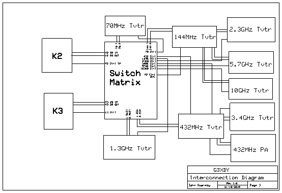
Figure 2 Overall Switch Box
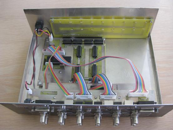
Figure 3 Switch Matrix Board
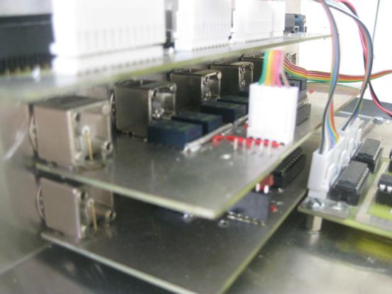
Figure 4 Rear Panel View