432MHz
Transverter
Introduction
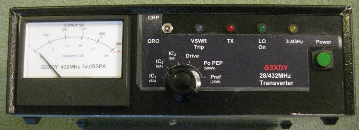
I have used a Yaesu FT736R on 432MHz for for more than 20 years, but the 736R is showing its age with noisy gain control pots and some recent poor signal reports. Plans for a new transverter and SSPA had been on the drawing board for some time, but this had now become urgent.
SSPA
The SSPA is based on two Band IV/V TV transmitter modules,
the first driver module is a balanced amplifier from the 1mW (0dBm) level to
about 25W operating in Class A. The second module is a PA with 6 Ericsson
devices, with 3 quadrature amplifiers running in parallel, rated for
Transverter
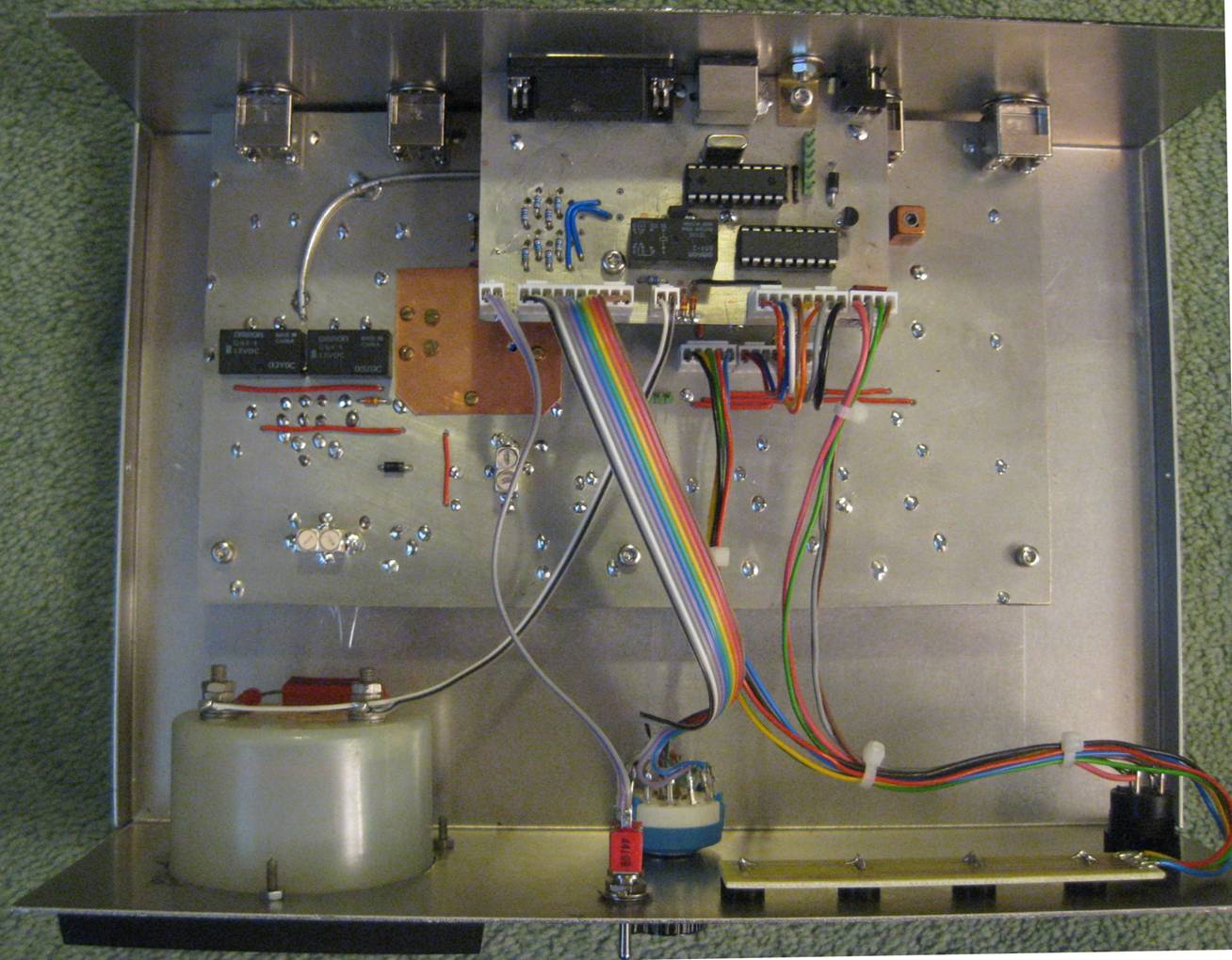
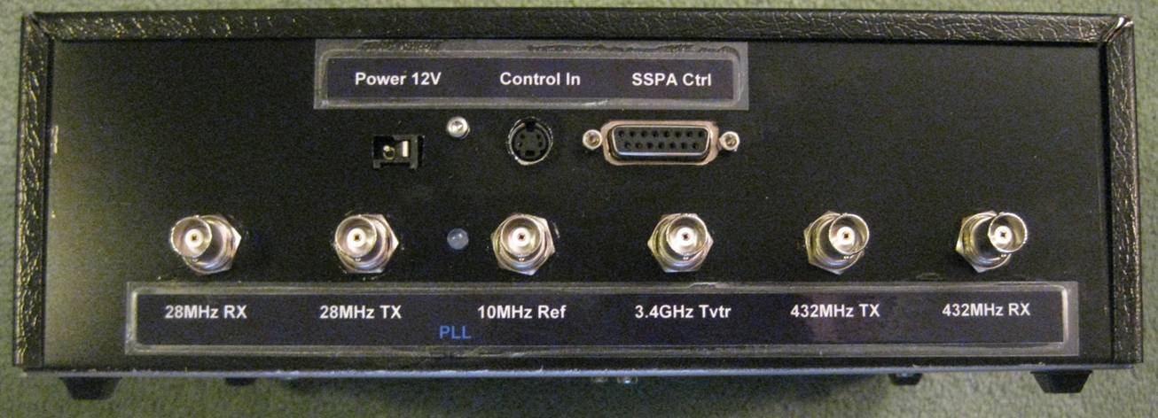
The new transverter is designed to work with the Elecraft K3 via the switchbox described elsewhere. The switchbox provides control signals that are used to enable the 404MHz LO when 432MHz or 3.4GHz is selected, transmit/receive switching and 3.4GHz transverter selection. The 28MHz transmit and receive IF signals are also routed via the switchbox. The transverter LO uses a 101MHz VCXO to a design by DF9IC which is phase locked to a 10MHz reference using an Analog Devices ADF4111 PLL operating with a 1MHz comparison frequency. A 12F508 PIC looks after loading the PLL with the right data when the LO is powered up. Two x2 multiplier stages take the LO to 404MHz, where it is buffered by a MAV-11 and fed via a 7dB pad to the mixer, a RMS-2LH type. The IF port is terminated by a T type diplexer and low pass filter and switched between receive and transmit. An IF post amplifier is not required on receive.
The first signal frequency selectivity is provided by a 2 chamber helical filter immediately in front of the mixer. From here the signal is switched to a BGA616 MMIC amplifier on transmit, followed by a SAW filter centred on 434MHz with 7MHz bandwidth. On receive the signal coming in from the masthead preamplifier enters via another similar SAW filter and is amplified by a SPF5043Z low noise MMIC.
Overall noise figure of the transverter is 4.5dB, which is dominated by the SAW filter loss. With 20dB masthead preamp net gain the overall system NF is about 0.6dB. The maximum transmit output is +7dBm (5mW) which will fully saturate the SSPA.
The output/input can also be routed to a 3.4GHz transverter. This transverter needs about 250mW of 432MHz drive, so a further amplifier is included using a SXA389B MMIC mounted on a commercial PCB which gives 300mW at the transverter socket. The transverter IF feed includes DC control of its T/R switching and a diplexer to pipe 10MHz to the masthead for locking the 3.4/5.7/10GHz transverters in due course.
Control
Control of the transverter is managed by a PIC16F628A. This looks after sequencing and controlling all the DC supplies to various stages and to the masthead preamp, through an 8 way high-side switch UDN2981A. The controller is on a separate board to minimise RF noise injection into the transverter. The multiplier resistors for the meter monitoring the PA currents are also located on this board, and a relay to switch the meter to monitor the 9cm transverter output is included.
Firmware
The firmware was written in assembler and then built and tested using MPLAB-IDE tools. The firmware structure is as follows:
Initialisation
On boot up the 16F628A sets up internal register options, disables interrupts and the comparator, and defines which pins are inputs and outputs.
The processor then calls the input routine.
Input
Routine
The input routine is looking for state changes on Port A which includes the input lines from the switchbox, and if a change is detected then a 1mS persistence check is undertaken to mask out noise. If there is no change or it does not persist then the processor continues to poll the inputs.
Output
Routine
If an input change does persist for more than 1mS then the output routines are called, starting with setting or clearing the SSPA TX enable bit, then setting up the Port B bits needed to apply +12V to all the circuits required. When going from receive to transmit there is a 30mS delay before power is applied to the transverter transmit amplifier to allow the antenna changeover relay to operate fully before RF appears. There is a similar 30mS delay when returning to receive.