2.3GHz Transverter and SSPA
Previous System
My old 2320MHz transverter was purchased
as a set of kits from G8LMW way back in 1985. Over the years various valve PA’s
have been used, from G3VVB style 2C39 cavities to a K9EK cavity, which produced
about 50W. An upgrade to all solid state took place in 2003, with the addition
of a driver amp based on a modified PCS1900 bipolar amplifier, and a PA using
an MRF21120 based on an Ericsson board. On a good day this would give over 100W
output.
This system had a number of drawbacks. The receive strong signal handling was
poor, even with extra filtering added there was severe intermodulation between
the 13cm beacon at Martlesham and a 2.1GHz UMTS transmitter about 300m south of
my QTH which made some southerly beam headings unusable. The filtering on
transmit also left something to be desired, with limited rejection of LO and
image signals. Frequency stability was marginal and this was one of the few
LO’s in the station not locked to a 10MHz reference.
New System
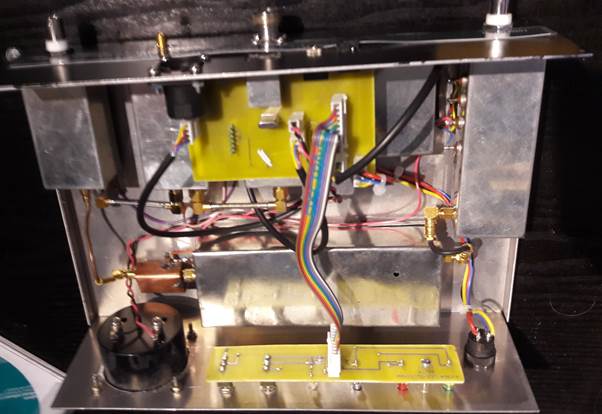
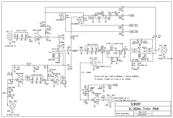
I was fortunate to acquire a number of ex-Lucent base station parts, which included an iPAM UMTS power amplifier. G4BAO and G4DDK had successfully got this model to work on 2.3GHz without modification with >250W output. I decided to use this PA with a new transverter using modern devices and designed for good strong signal performance and out of band rejection on both transmit and receive. This was helped by acquiring a number of miniature ceramic filters made by Lark Engineering intended for Sirius receivers. These have a pass band centred on 2335MHz but work fine on 2320MHz and are just starting to roll off on the LF side at 2300MHz. The new transverter would operate not only on the usual 2320MHz band, but also on the UK only 2300-2302MHz segment.
Local Oscillator
A dual LO was designed based on the DF9IC circuit I have used elsewhere, using two J310 FET oscillators, one on 90.666667MHz and the other on 89.833333MHz. These share a common output buffer FET to drive the following multiplier stages. The ADF4111 PLL chip has a differential RF input so the oscillators each feed one input line. The PLL registers are reloaded when the crystal oscillator power is switched over to lock the appropriate crystal to the 10MHz reference.
Multiplier Chain
This is an old G4DDK004 board with the oscillator stage reconfigured as an amplifier/buffer for the +3dBm drive from the DF9IC oscillator. Despite careful tuning it was only possible to get a little over 0dBm output from the multiplier board in a stable manner, so a small amplifier using an SPF5043Z MMIC was added to obtain +9dBm of LO at 2156MHz or 2176MHz.
Mixer
The mixer is a Mini-Circuits ADE-3G+ which is well suited
for the 13cm band. The IF port is terminated in a twin tee diplexer which looks
like 50 ohms on both input and output, and there is also an open circuit stub
that reduces any LO feedthrough into the 144MHz IF output. The stub capacitance
resonates at 144MHz with a 470nH RF choke. When in the unpowered state the
mixer is protected from transmit drive being inadvertently being applied by a
bypass relay that normally inserts a 30dB pad in line. When powered up on
receive the relay operates to provide a straight through connection with just a
pair of back to back silicon diodes as protection. On transmit the 30dB pad
reduces the drive to the mixer to about 0dBm.
The RF port of the mixer is directly connected to a Lark filter block. This
reduces the levels of the unwanted sideband and LO feedthrough by about 40dB
compared with the wanted signal.
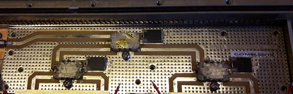
Transmit Amplifier
The mixer connects to the transmit amplifier which
includes a transmit/receive relay to select the transmit or receive amplifier
blocks. On transmit the signal passes to a SPF5043Z MMIC and then into another
Lark filter, followed by an MGA-31289 medium power MMIC which produces about
50mW of output. In practice only about 10mW is needed to fully drive the SSPA,
so this is followed by a 6dB pi attenuator to match the drive level required.
Receive Amplifier
The receive amplifier follows a mast head preamp using two ATF54143 stages, so
there is plenty of gain available to overcome a moderately high transverter noise figure. The receive signal first goes
through a Lark filter that helps reject out band signals such as the UMTS base
station at 2.1GHz, and then into another MGA-31289 medium power MMIC. Despite
being capable of 200mW RF output, this device offers a NF of 2dB at 2.3GHz,
with an output third order intercept of +42dBm, so is well suited for use in
this role. With under 2dB loss in the Lark filter the transverter
NF is approximately 4.5dB. The net gain of the masthead amplifier and its
feeder is 22dB, with a NF of 0.77dB, so the overall receiver NF is only
marginally worse at 0.81dB
Control
The control of the transverter is
done by a PIC16F873A which also controls and monitors the SSPA.
The software polls the transmit/receive line and the LO enable line to
determine what state the transverter/SSPA should be
in, and monitors reverse power on transmit to trip the SSPA if the VSWR is too
high. The PIC also drives the front panel meter showing either forward or reverse power in dBW.
Masthead preamp
control
The masthead preamp power controls the relay switching between 1.3GHz and 2.3GHz at the masthead, as well as T/R switching for 2.3GHz. When 2.3GHz is not selected then no power is applied to the masthead interface and the main low loss feeder is connected to the 1.3GHz system. If 2.3GHz receive is selected then 21.5V DC is applied to the preamp power line which operates the 2.3GHz transmit receive relay to connect the antenna to the preamp, which is also powered up. On switching to transmit the voltage is increased to 26V which operates the 1.3GHz/2.3GHz switch, drops the 2.3GHz transmit/receive relay back to the transmit position and switches off the preamp. The transverter includes a DC-DC step up converter to power the relays independent of the 28V supply to the SSPA.
SSPA
The iPAM SSPA uses four MRF6S21100 devices in the output stage with Xinger 3dB hybrid couplers on the inputs and outputs. The XC2100A-03S couplers are only rated for 145W average power, so the final output coupler was removed and an XC2500A-03S rated at >200W average was mounted in its place, with the aluminium cover plate milled out to take account of the greater height of the new coupler. The output line and circulator were also removed and a new directional coupler and pair of power detectors installed in their place. The power detectors sense forward and reverse power in a short piece of RG402 line filed to expose the internal insulation and soldered to the main RG402 line that has been similarly filed. This makes a directional coupler with about -46dB coupling. The RF power is detected by AD8312 power detector devices that give a linear voltage output for a log input power scale, so the power meter on the transverter is calibrated in dBW and is driven by a linear conversion function in the control PIC.
The iPAM has T/R switching implemented by enabling the bias for the PA and driver devices on transmit, under control from the transverter. The same control line also switches the cooling fans into transmit mode.
Cooling for the SSPA is provide by four 12V DC fans that normally run slowly in series on 28V when on transmit. This is sufficient cooling for low duty cycle operation. If the heatsink temperature exceeds 50 degrees C then the fans are reconfigured for full power and run in pairs, and will revert to slow speed operation when the temperature falls below 48 degrees.
The iPAM output connector is SMA which is a bit marginal at the 250W level, but there is not really enough room to replace it with an N type. The output cable to the main feeder relay is Sucoform 250 about 0.5m long. This has enough loss to get noticeably hot on transmit, losing about 15W of power before the RF gets to the main LDF5-50 feeder. The total feeder loss is calculated to be 1.8dB, so for 250W output at the PA, about 180W should arrive at the antenna.