Solid State Circuits 15 -
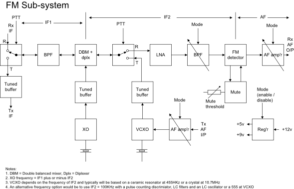
The following block diagram shows a suggested design overview for a solid state analogue FM adaptor that could be added to most transceivers assuming that the existing IF filtering can be modified to add one or more suitable bandwidth filters. Existing SSB or narrow AM filter will be unsuitable for FM use.
25KHz channel spacing requires a filter 3dB bandwidth of +/-
20KHz channel spacing requires a filter 3dB bandwidth of +/-
12.5KHz channel spacing requires a filter 3dB bandwidth of +/-
This module has a bidirectional mixer to convert the transceiver IF (IF1) to and from 455KHz (IF2) using an appropriate frequency crystal oscillator (XO).
The two variable gain AF amplifiers and IF2 band pass filter are intended to provide control of the receive and transmit AF levels and receiver bandwidth respectively for each different channel spacing.
A speech processor and filter will be required (not shown above) to ensure that the maximum deviation level for each channel spacing is never exceeded. See Semiconductor Circuits elsewhere on this site.
As mentioned in the diagram notes an alternative IF2 of around 100-
For receive only applications the transmitter and changeover components may be omitted.
A circuit of an FM adaptor will be added in due course.