Control Circuits
There are many methods that may be used to control internal or remote circuits from a front panel or even a remotely sited control. For hard wiring I prefer to use pull-
Care is needed with controlling remote or distant circuits to minimise the risk of damage from induced energy from adjacent equipment/control lines.
Shown below are a number of simple circuits in use in my various communications units. Diode D1 allows switch S1 to control a number of the same polarity but dissimilar voltage circuits at the same time.
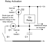
1. Control of low power relays used in band switching this would usually be two relays, one on the input and one on the output of each band filter. The series diode D1 is not required if all relay circuits controlled by S1 are powered from the same voltage supply line.
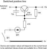
2. Control of a low power supply line to an oscillator, electronic filter etc. As shown the circuit will provide up to 10mA and the voltage drop across the device will be up to about 0.2V.
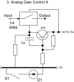
3. This circuit shows how to control an analog switch like the 4066 from an an active low switch S1. The PNP transistor, which is used as a DC inverter could be replaced by another analog switch as shown in circuit 4.
4. This circuit shows how to control an analog switch like the 4066 from an an active low switch using another analog switch as an inverter.
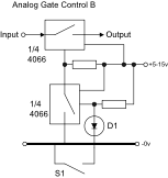
5. This circuit shows how to format analog switches to provide high attenuation on the off state.
However, there is an inherent limit to the amount of attenuation that can be achieved due to the cross talk between individual switches on the IC substrate and little can be done about that in the 4066 quad analog switch.
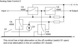
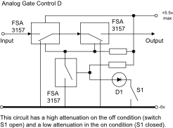
6. This circuit offers a much higher attenuation in the off state by using packages containing just one analog switch like the FSA3157 so no cross talk can take place. When the upper analog switches are in the off state the common centre connection is grounded so providing a low impedance path to any signal leakage across the two series gares.
The lower analog gate is used as a DC inverter. The resistor values may be relatively high and RF decoupling is not shown for simplicity. Note the lower maximum supply line voltage compared to the previous examples.
Do refer to the data sheets for the maximum allowable signal voltage.