A transmit mixer-amplifier for the 13cm band
G0ORY-005
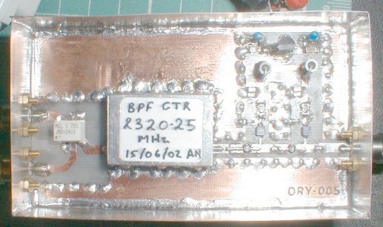
This unit was developed to enable an MMDS downconverter to be turned into a 13cm
transverter. When designing this unit, there were three aims - Low cost, Ease of
alignment, and a small size. The unit described herein is built on standard double-sided
epoxy-fibreglass pcb material, uses an SMD balanced mixer salvaged from surplus equipment,
a three pole bandpass filter made from tinplate and some scrap lengths of .141 semi-rigid
coaxial cable, which is integrated onto the PCB, and a two stage MMIC amplifier using the
easily and cheaply available MAR-6 (MSA-0685 in the author's instance) drop-in
MMIC amplifiers. Alignment is facilitated by a once only access to a tunable wavemeter,
spectrum analyser, or power meter with a pre-aligned 2320MHz bandpass filter placed in
front of it. Once the filter is peaked in the 2320MHz band, no further adjustments are
necessary. Drive requirements are in the order of 0dBm at 144MHz, and approx +4..+7dBm of
2176MHz local oscillator. Output is typically +10dBm at signal frequency, which is ample
to drive a companion PA to 1W (+30dBm) and above.
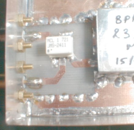
The mixer used in this unit is a JMS2411. This was made by Mini-Circuits as a special to
be used in the United Kingdom IONICA WLL (telephone) service in the 3.4GHz Band.
Originally the Mixer was used with a 2.4GHz LO, and 1GHz IF to produce the required 3.4GHz
out of the RF port. Initial tests illustrated well that the mixer was amply capable of
good results at 2.3GHz, with a 2176MHz LO, and 144MHz IF drive. Therefore the PCB is
designed with this mixer in mind, the surplus equipment being readily available. However
other mixers may perform amply well, and possibly share a common pinout. Inspection of the
PCB will reveal the layout for those planning to substitute other SMD mixers. It would be
interesting to know how other MCL mixers work out - the author awaits your exploits
with open ears.
Filters at 2.3GHz need not be expensive, time consuming or hard to
produce. A filter was developed, using ordinary tin-plate (K&S metals) which is also
used to fabricate the outer casing of the module. A template is provided to produce the
'carrier' that holds the resonators and tuning capacitors - these are merely lengths of
.141 semi-rigid coax, with the inner conductor made to effect a high-Q capacitor for
tuning, by varying the depth of insertion of the inner wire into the resonator. Refer to
the separate text dealing specifically with the filter's construction. The construction
works extremely well, and after the author fabricating two of these units, it was felt
that these are easily reproducible. The author used a vernier caliper guage to carefully
measure dimensions (tolerance to 0.5mm should be the maximum allowed, but get the nearest
you possibly can!). In this instance, the filter is constructed and the carrier soldered
directly and evenly onto the main PCB. Coupling into and from the filter is from stripline
on the PCB. Short L shaped silver plated probe wires are soldered to the input and output
resonators, and then to the stripline on the PCB. Good joints and accurate, symmetrical
placing of the carrier about the pcb are important.

Here is the swept trace from the bandpass filter (in fact the trace
shows the response through the entire assembly). The detector is a negative type, so the
'peak' is in the downwards direction. In the centre of the peak is 2320MHz. Half way up on
either side of the peak is at around plus or minus 10MHz. I guess this is the 3dB point
for the filter, but that will be confirmed by using a power meter and manually stepping
the sweep instead. Notice that the peak isn't as well-defined as the 23cm unit (G0ORY-005A
- or the 'stretched PCB') - we're pushing the limits of the simply constructed filter
here. A filter for 9cm would be worse than this, so I guess it's going to be pipecaps on
the next band up.
Construction details for the 13cm Bandpass Filter
Once the filter is installed on the PCB, further vias are drilled around
the perimiter of the filter itself as close to the perimeter of the filter carrier as is
practicable. Then solder in the via wires. Good soldered joints are a must.
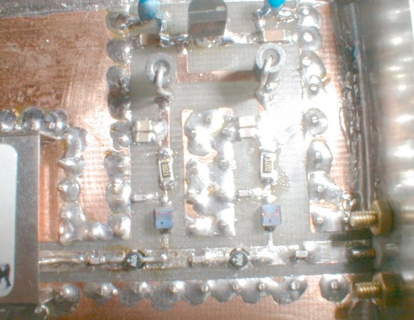
The two stage MMIC amplifier is constructed to a standard pattern, and has extensive
decoupling to prevent rf oscillation, feedback, mutual effects (read HP data sheet) etc.
The 78L06 regulator has both a 0.1uF SMD capacitor and a 1uF tantalum capacitor on each in
and out leg. Supply to the 78L06 is brought out from the underside of the PCB and through
a 1nF feedthrough to the outside world. It is important to solder correctly the SMD
capacitors onto the board. The 22nH RFC's for the MMICS were in the Author's instance
salvaged from the IONICA motherboard, and reused. 0805 size capacitors should work well
for the 50 ohm line portion, however 0603 types are the authors preference, and were used
in the prototype. The author used 10pF for coupling and decoupling, although 4.7pF is a
better value at 2320MHz (see HP datasheet). A mixture of 0805 and 0603 sized parts were
used for decoupling, and the 0.1uF capacitors around the 78L06 are 1206 style cases -
mainly for the higher voltage rating. All capacitors are manufactured by PHILIPS and are
standard parts (NP0 dielectric). The constructor should be able to use whichever is to
hand, but 1206 style cases are not optimal for use at 13cm on the 50 ohm portion, or for
the first decoupling capacitors. The MMICs are installed last after prechecks (see further
below).
Construction of the casing surround is from a single sheet of tinplate,
scribed and cut 30mm in width. Two pieced from the specified sheet are required, and then
marked and drilled for the SMA connectors and feedthrough, then formed into two L shapes
and soldered squarely to the PCB. The PCB must have a good solder fillet all the way round
the top and bottom sides to the tinplate walls - tack soldering is not good enough, both
strength and RF performance are increased by ensuring good soldered seams.
When the unit is boxed and connectors installed. Power up and check the voltages at the
MMIC output pads are correct. Then install the MMICs using antistatic precuations. Fold
the grounding wires on each MMIC downwards and insert the MMIC into the board. It should
sit snug, and then turn the case over and fold over the grounding wires to the groundplane
on the pcb, soldering in place. Then turn the board over to the component side again and
solder both input and output using a minimum of solder, and heat dwell.
Once done, power up and check the voltage is at approximately 3.5V on both MMIC output
pads. Any deviations from this, remove power and check your work. Check also the voltages
on the input pads - these will be around 1V (due to internal networks within the MMIC).
Low or no voltage implies a faulty MMIC or short - check your work throroughly.
One satisfied that both MMICs are okay, apply the LO and drive to the board, watching
carefully the output on a wavemeter tuned to 2320MHz, or spectrum analyser (recommended).
Failing this it should be possible to use a sensitive power detector (HP432) with a
2320MHz bandpass filter of known bandwidth (but not so wide as to allow the LO at 2176MHz
or the image frequency at 2032MHz through) inserted before it's detector. Peak up the
filter for maximum output, ensuring the insertion wires are making a good ground contact
with the filter carrier at all times (slight downward pressure on all three whilst tuning
is recommended, although somewhat fiddly) iterating the process until no more output can
be gained. Then solder the tuning wires to the tinplate carrier and crop. Double check
output, and see that this has not changed significantly. Also then check for output at the
image frequency. This should be minimal. The LO power emerging from the balanced mixer is
extremely small due to good balance of the mixer itself. You should see close on +10dBm of
the right signal at the output. That completes the alignment of the entire unit. The
filter is wide enough to allow large excursions within the 13cm SSB portion without losing
output.
It is then time to find the 1dB compression point for the transmit mixer. With a spectrum
analyser or accurate power meter this is simplified. A useful rule of thumb for
constructors without ready access to either is to advance 144MHz drive from a minimum
watching the output creep up on a diode detector. Note the point where the power output
from the unit stops increasing, or even starts to decrease, then back off around 10% from
this to give the optimal drive level. Overcompressing the drive will increase width and
splatter, an on-air check with another station carefully monitoring for these ill-effects
is the bare minimum requirement. Despite the 13cm band being rather somewhat unoccupied,
it is still desirable to keep one's nose, and therefore one's emissions clean!
Back to the microwave
radio page