Linear power amplifier with switching-mode modulator
File:   C:\myhome\mf\SwitchMode_Linear.html
Author: Wolfgang 'Wolf' DL4YHF
Date:   2014-01-02
Motivation
Several amateur radio modes (like binary PSK with envelope shaping) require a 'linear' power amplifier.
For some other modes, even those with the ancient on/off keying like CW (Morse),
it's also desirable to avoid hard keying to keep the sidebands (click spectrum) reasonably low.
The author's previous amplifier (for MF) used cheap switching-mode MOSFETs for that purpose,
biased into the 'linear' region with approximately 0.5 A quiescent current,
and moderately driven for a maximum power output of 50 Watts.
That amplifier's efficiency was below 60 %, which is only acceptable at low power levels.
- Note:
- Some barely successful experiments to increase the efficiency of the old PA are in ..Mittelwelle\pa_modifikation_2013.htm).
When the ERP at DF0WD appeared to be well below 0.5 Watts (by means of fieldstrength measurements,
and comparisons with other MF stations), a new 'linear' (power amplifier) was built as a proof of concept.
The choice was that, instead of operating the MOSFETs in the 'linear' region and adding a large heatsink,
the RF power output stage should run in switching mode, and produce a maximum power of approx. 150 Watts.
The maximum DC input current should be around 15 A (at 13.8 V) to have some margin for the IC-706 (exciter) from the
station's '20 Ampere' power supply. With approx. 200 W DC input power, and 150 W RF output,
the design goal was "at least 75 %" (later, 87 % were achieved, even with non-optimal parts from the junkbox).
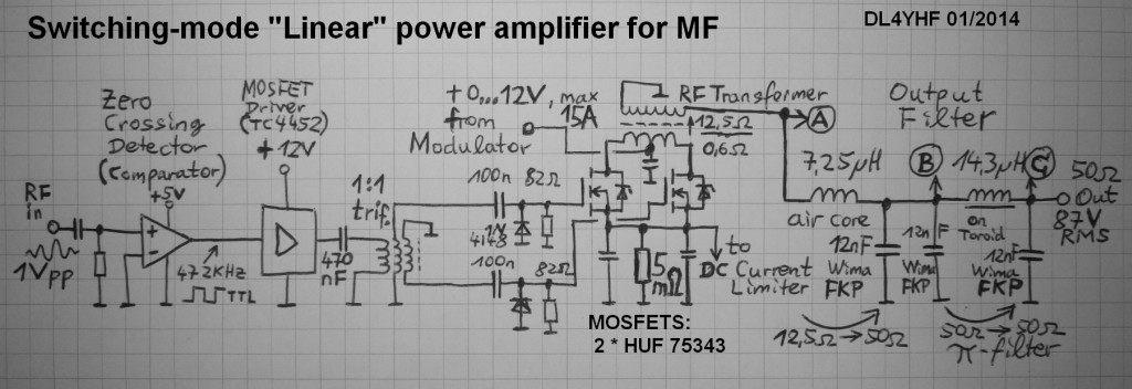
The 'new' PA (put into service in January 2014) consists of...
- a precision rectifier (here: a synchronous rectifier, driven by the phase signal which also drives the MF output stage);
- a zero-crossing detector which produces the 'carrier phase' for the RF;
- a power modulator which provides the "DC" voltage for the final RF stage, output voltage range from 0.2 to 13.8 V;
- switching mode power amplifier with two alternatively driven MOSFETs;
- an RF transformer to match the very low drain output impedance (less than 1 Ohm) to 12.5 V
(so the following lowpass filter doesn't have to carry the full drain current)
- harmonic filter, protection circuits against high VSWR and excessive drain current, RX/TX switching, etc.
Preview of the power modulator, and RF final stage (details further below):
The switching-mode 'linear' PA was built from various 'modules' on a large copper-clad board (see photo below).
The entire base board is at ground level, and there are no traces etched (or cut) into it.
All modules (like sync rectifier, auxiliary negative voltage supply, PWM, SWR sense, current sense, protection)
are built on smaller, individual PCBs.. in fact, the 'PCBs' are neither 'printed' nor etched; the copper traces were cut with a sharp tool.
Photograph of the PA in an 'early stage', running in a two-hour stress test
(during which much water was boiled to cool the dummy load resistor on the left side) :
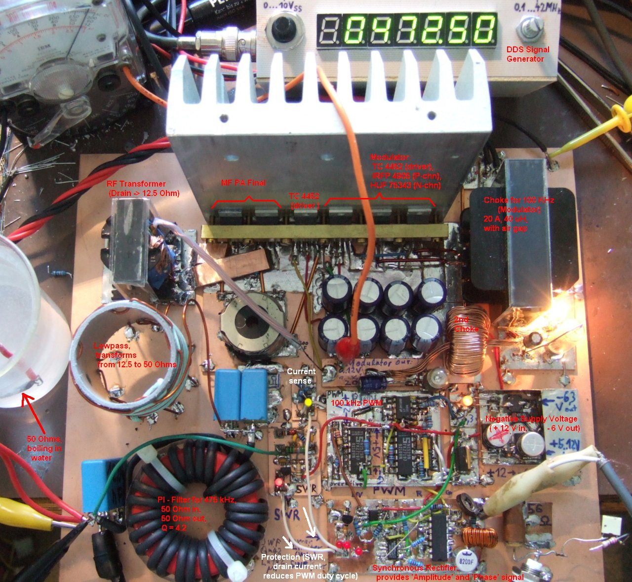
Click on the image for a full-screen view
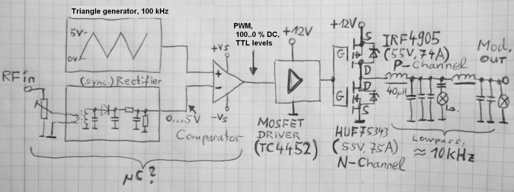
This modulator provides a variable DC supply voltage. In the original prototype, it uses a pulse-width modulator (PWM) at 100 kHz.
The lowpass-filtered output (at the right side of the principle shown below) delivers 0.1 to 12 (or 13) Volts DC, and up to 15 Ampere.
Power modulator principle
In the original design, the cutoff frequency for modulator's low-pass output filter was 20 kHz, and two L-C stages were used.
When tested with a highly linear amplitude modulator, and fed with 'Hi-Fi' audio, the signal (monitored with a AM receiver
with sufficiently wide filter) was also 'Hi-Fi'. Possibly a bit over-engineered for a 3 kHz SSB signal, or CW, or PSK31;
but the delay through the amplitude modulator should be kept as low as possible, to avoid distortion
which would be caused by different delays between amplitude- and phase- signal
when recombined in the RF final stage.
- Note:
- If, as originally planned, a microcontroller was used to generate the amplitude (envelope) and phase-signal,
the different delays could be compensated by software, and much simpler lowpass could be used if the modulator frequency was,
for example, an integer fraction of the 'radio' frequency...
The incandescent lamps in the modulator's output filter serve different purposes:
- dampen the L-C filter's 'Q', to avoid ringing near the cutoff frequency
(if the modulating signal ever gets close to it, which is unlikely for CW, PSK, and even 3 kHz SSB)
- provide an 'optical feedback' for the operator
- indicate if the SWR-protection or drain-current-limiting control loop oscillates
(as it did, during the first experiments, before modifying the loop filter... ToDo: place a link here)
The complementary design of the modulator's final stage (using a P- and an N-channel MOSFET),
along with a MOSFET's ability to conduct current in both directions (drain to source, source to drain)
allows the modulator to drive non-resistive (i.e. reactive) loads.
In other words, the modulator can not only 'source' current, it can also 'sink' current
regardless of whether the P- or N-channel transistor conducts. While the transistor conducts,
any current flowing in the 'reverse' direction will not flow through the (lossy) body diode,
but through the drain-source path which has an Rds_on of 9 to 20 milliohms.
- On this occasion:
- Rds_on of the P-channel transistor is 20 mOhm, which causes a voltage drop of up to 0.3 V,
or a power loss of ~ 4.5 W. Thus two P-channel transistors connected in parallel would let the heatsink run cooler.
The HUF75343 is specified with Rds_on = 9 mOhm, so it doesn't pay off to use two in parallel for the modulator.
In the prototype, the pulse width modulator is a simple triangle wave generator, running at 100 kHz (fixed), output ramping up and down
from 0 to 5 Volts. The triangle wave is compared with the output of a high-precision synchronous rectifier.
ToDo: Add details / circuit diagram of the PWM unit here ...
This is just a simple zero-crossing detector for the RF input signal. To ensure a perfect 50 % duty cycle (for the RF final stage,
but also for the synchronous rectifier), the RF input (here: 475 kHz +/- x) passes through an LC bandpass filter before being fed
to a high-speed comparator. This way, the distorted output from an old IC 706 (used as 'exciter' on MF) doesn't matter too much.
The output of the high-speed comparator is fed to the RF stage's MOSFET driver - see RF final stage.
Since the power modulator, in combination with the pulse width modulator provides a dynamic range of
20 * log ( 13 Volt / 0.1 Volt ) = 42 dB
,
it 'would be nice' if the RF rectifier (which provides the 'amplitude' aka 'envelope' for the modulator) had at least a similar
dynamic range. But even with Schottky diodes, the linearity wasn't very good.
So a synchronous rectifier was used in the prototype, which consists of an analog switch (controlled by the same 'phase channel'
which also drives the RF final), and a few opamps for an active lowpass filter.
To be continued ...
To keep it simple, a simple class-D amplifier with two N-channel MOSFETS (HUF75343, 75 A, 55 V, Rds_on=9 mOhm) was used.
At a supply voltage of ZERO to approximately 13 Volts (provided by the power modulator), the drain load impedance must be low,
thus an efficient way to transform this into a larger impedance was required. A simple toroid transformer,
wound with round copper wire, or large multi-stranded HF litz wire, was not sufficient because the stray inductance
was too large (causing low drain current, but 'nasty voltage spikes' on the drains).
The solution was a modified transformer from a switching-mode 'PC' power supply, which had carefully been 'roasted' (!)
on an electric cooker to take the two glued ferrite parts apart.
Then the original turns were removed, and replaced by multiple layers of 19 mm wide copper foil (the adhesive stuff used
to cure EMC problems), insulated by covering both sides of the copper with adhesive tape ("Tesa-Film" in Germany).
- Primary :
- 2 * 3 turns, i.e. 6 turns total with center tap for the DC feed from the modulator.
- Secondary:
- 12 turns total,
here: made of 2 * 6 turns, interleaved with the primary to reduce stray inductance.
This way, at a drain current of 15 Amperes, an impedance of approximately 12 V / 15 A = 0.8 Ohm
would be transformed into 0.8 Ohm * (12 turns / 3 turns)^2 = approx. 13 Ohm.
For further calculations, assume an impedance of 50 Ohm / 4 = 12.5 Ohm at this point.
The next stage is a lowpass filter, which transforms 12.5 to 50 Ohm, and removes the strong harmonics.
Designed using DL4YHF'c CalcEd, the closest 'norm value' for the capacitor was 12 nF (ZC = -j * 28.8 Ohm);
and the coil (7.2 uH, ZL = j * 21.65 Ohm) was build as a single-layer cylindrical coil
using the excellent 'Single-Layer Helical Round Wire Coil Inductor Calculator' by Serge, ON4AA,
at http://hamwaves.com/antennas/inductance.html.
RF final (principle)
The sources of the two MOSFETs are connected to ground via a 5 milliohm resistor (RF bypassed by capacitors),
which produces a DC voltage drop of 75 mV at the maximum current. Not shown in the above schematics for clarity:
A 5-Volt powered 'rail-to-rail' opamp amplifies this signal for the protection circuit, which reduces the power modulator's
PWM duty cycle (and thus the DC supply voltage for the RF final stage) if the DC current exceeds the maximum.
Actually, this 'Current Sense' resistor is made of a thin piece of sheet metal.
The lowpass is followed by a simple PI filter (50 Ohm in, 50 Ohm out).
The PI filter is also part of the VSWR measurement / protection circuit, by comparing the phases and voltages at the in- and output
of the PI-filter (points 'B' and 'C' in the diagram above).
It's a quite conventional design (as can be seen in many 'class-D' amplifiers), except for the supply voltage
for the final stage, varying from zero to the maximum DC supply voltage. Thus, the tricky part is not the 'RF part'
of this amplifier, but the switching mode power amplifier (including the precision rectifier, pulse width modulator, etc).
To be continued ...
To be continued ......