
| The Battery Guardian Don't get caught with a flat battery; this easy-to-build circuit can cut off the power to a 12V fridge or car stereo system if the battery voltages drops below critical level. By John Clarke |

Operation on 12V is fine when the motor is running and battery charge is maintained but if the fridge is allowed to run for too long when the motor is stopped, it can flatten the battery in a relatively short time. This is where the Battery Guardian comes into play. It monitors the battery voltage and disconnects power to the fridge before the battery becomes too flat to allow the engine to be started again.
| MAIN FEATURES
|
Note that some fridges already have a low battery cut-out that prevents operation if the battery voltage goes below 10.5V. The cut-out is included for two reasons. One is to prevent the battery from being discharged to the point beyond which the battery life is reduced. The second is to prevent the fridge motor from stalling since it would not be able to drive the fridge pump at such a low voltage.
However, at 10.5V, no vehicle battery could start the motor and therefore you could easily be stranded way out in Woop Woop.
By contrast, the SILICON CHIP Battery Guardian disconnects the power when the battery voltage drops to about 11.5V. At this voltage, the battery should still have sufficient reserves to start the engine but you can set the cut-out voltage higher or lower to suit your vehicle.

The SILICON CHIP Battery Guardian has to operate without causing any significant additional current drain from the battery. If it did have a significant current drain, it would become part of the problem rather than being the solution. This fact means we cannot use a relay to control the power switching. A suitable automotive relay would draw some 120mA continuously when activated so clearly we had to rule this option out.
Instead of a relay, the Battery Guardian uses a power Mosfet and this cuts power consumption dramatically. In fact, the whole circuit draws an average current of less than 2.5mA.
Fig.1 shows the circuit. It uses three low-cost ICs, the power Mosfet and not much else.
Mosfet Q1 provides the switching for the 12V rail (ie, between the 12V IN and the 12V OUT). This rail is fused using fuse F1 (10A), to protect against short circuits on the 12V output.
High side switching
One of the problems with using a Mosfet to switch +12V rail is that its Source and Gate electrodes cannot be connected to the 0V side of the supply. Instead, we are using the Mosfet as a "high side switch" (ie, switching the positive supply rail). This means that the gate voltage must be referenced to the source electrode of the Mosfet which rises to almost the full positive supply when the Mosfet is switched on.
Hence, we need to generate a gate voltage for the Mosfet which is tied to its source electrode and isolated from the 0V line. And Q1 needs a gate voltage which is at least 10V above its source in order to switch fully on.
This voltage is provided using an oscillator circuit (IC1) which drives transistor Q2 and a small step-up transformer, T1, wound on a ferrite toroid. The output of T1 is rectified using D1 and a 0.1μF capacitor (for filtering) to derive a signal which is fed to Q1's gate.
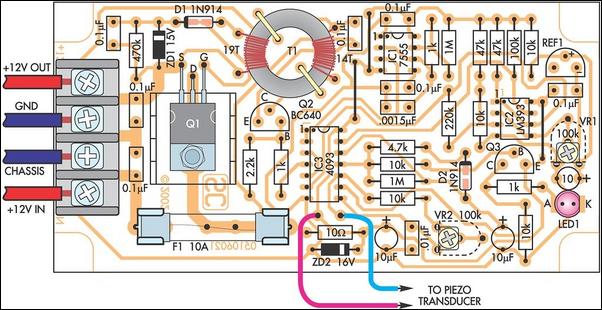
IC1 is a CMOS 7555 timer which is connected to operate in astable (continuous) mode. Its frequency of oscillation is set by the .0015μF timing capacitor on pins 6 & 2 and by the associated series 1MΩ and 1kΩ resistors on pin 7.
Using the timing components shown, IC1 runs at about 1kHz, with the charging time (.0015μF x (1MΩ + 1kΩ) x 0.693 = 1.04ms. By comparison, the discharge time is very short, around 1ms, since the 1MΩ resistor is not involved.
The pin 3 output of IC1 is high while the timing capacitor is charging and low when discharging (ie, the output is a pulse waveform with a high duty cycle). This pulse signal is inverted using NAND gate IC3a and inverted again using IC3b (assuming that pin 6 of IC3b is high).
IC3b drives the base of transistor Q2 via a 1kΩ resistor. As a result, Q2 switches on for about 1ms every 1ms and pulses the primary of transformer T1. The secondary of transformer T1 drives diode D1 and its associated 0.1mm filter capacitor and the resulting DC voltage turns on Mosfet Q1.
Zener diode ZD1 limits the gate voltage applied to Q1 to a safe value - ie, to no more than 15V between gate and source (or 27V above ground).
Q1's "on resistance" is typically .02Ω and this means that it will dissipate about 0.5Ωwhen supplying 5A to the load (eg, fridge or whatever). In addition, as the Mosfet turns off, it dissipates power as its gate voltage falls. In fact, the dissipation will be higher during this turn-off period (about 50ms), as its "on resistance" increases. For this reason, a heatsink has been used to ensure that the device runs cool.
Mosfet Q1 is switched off (to cut the power to the load) when pin 6 of IC3b is pulled low. This sets pin 4 of IC3b high and so transistor Q2 turns off (and remains off). As a result, the 470kΩ resistor between Q1's gate and source terminals discharges the 0.1μF capacitor over a 47ms period and the Mosfet switches off.
Voltage sensing
Pin 6 of IC3b is controlled by a voltage sensing circuit consisting of REF1 and comparator IC2a.
REF1 is a 2.5V voltage reference and is supplied with current via a 10kΩ resistor from the 12V rail. Its 2.5V output is attenuated by trimpot VR1 (which sets the cut-out voltage) and applied to the inverting input (pin 2) of IC2a. At the same time, the non-inverting input (pin 3) monitors the supply voltage via a voltage divider consisting of 47kΩ and 10kΩ resistors.
Normally, with a fully charged battery, the voltage on pin 3 is greater than that on pin 2 and so pin 1 is high. As a result, pin 6 of IC3b is also high and so IC3b gates through the pulses from IC1 to Q2, as described previously. The 220kΩ feedback resistor between pins 1 & 3 of IC2a provides a small amount of hysteresis, so that IC2a switches cleanly at the cut-out setting.
The resistors connected to pin 3 set the voltage at this pin to about 1/5Vcc (ie, one fifth of the supply voltage). This means that if we want Q1 to switch off at 11V, we have to set VR1 so that pin 2 is at 2.2V. When pin 3 falls below this voltage (ie, as the battery voltages falls below 11V), pin 1 of IC2a goes low and so IC3b blocks any further pulses from IC1 and IC3a.
As a result, Q2 remains off and so Q1 also turns off and disconnects power to the load (ie, the fridge).
At the same time, the low output at pin 1 of IC2a pulls pin 3 down to 1.86V, since the 220kΩ feedback resistor and 10kΩ resistor are now effectively in parallel. The voltage on pin 3 is now effectively 0.169 x Vcc, which means that the battery voltage must now go above 13V before the voltage at pin 3 equals the 2.2V at pin 2 and pin 1 switches high again.
Without the hysteresis provided by the 2.2MΩ feedback resistor, pin 1 would simply cycle rapidly between high and low as the battery voltage recovered each time the fridge load was removed.
Note that REF1 has a 10m F capacitor across it. That's there to ensure that REF1's output is initially low when power is first applied, so that pin 1 of IC2a is high. Pin 1 of IC2a will then go low again if the supply voltage is below the cut-out value set by VR1 but only when REF1's output has settled to its correct value - ie, after the capacitor has charged via the 10kΩ resistor.
Indicator circuitry
As well as controlling pin 6 of IC3b, IC2a also drives the inverting input (pin 6) of comparator IC2b. As shown, IC2b's non-inverting input is connected to VR1's wiper, which means that it is nominally at 2.2V.
When pin 1 of IC2a is high (ie, Q1 on), IC2b's output at pin 7 is low and so NAND gate IC3d and any following circuitry is disabled. However, when pin 1 of IC2a goes low (ie, to turn Q1 off), pin 7 of IC2b goes high and allows NAND gate oscillator IC3d to operate.
The feedback components between pins 11 & 12 and the associated 10m F timing capacitor set the frequency of the NAND gate oscillator. To understand how this works, just remember that the output of a NAND gate only goes low when both inputs are high.
Assume initially that Mosfet Q1 is on. This means that pin 7 of IC2b and thus pin 13 of IC3d are low and so pin 11 of IC3d will be held high.
Pin 12 of IC3d will also be high during this time, since the 10μF timing capacitor will charge via the 1MΩ feedback resistor. At the same time, PNP transistor Q1 will be off (since its base is held high by pin 11) and so both LED1 and the piezo siren will also be off.
OK, now let's see what happens when the Mosfet (Q1) switches off. When that happens, pin 7 of IC2b goes high and pin 11 of IC3d switches low. The 10μF timing capacitor now discharges into this low output via D2 and a series 4.7kΩ resistor until it reaches the logic low threshold of pin 12. When that point is reached, pin 11 of IC2b switches high again and recharges the 10μF capacitor via the 1MΩ feedback resistor, whereupon pin 11 switches low again.
This cycle continues while ever pin 13 of IC3d is high, with the 10μF timing capacitor charging via the 1MΩ resistor and discharging via D2 and the 4.7kΩ resistor (ie the capacitor discharges far more quickly than it charges). As a result, pin 11 of IC3d is high for about 10s and low for about 10ms during each complete cycle.
Each time pin 11 pulses low, Q3 turns on and briefly flashes LED1. It also briefly enables NAND oscillator IC3c (by pulling pin 9 high). This oscillator runs at around 1-2kHz (depending on the setting of VR2) and briefly drives the piezo siren.
As a result the piezo siren briefly "chirps" and the LED flashes once every 10 seconds to let you know that the power to the load (fridge) is "off".
Unlike NAND gate oscillator IC3d, IC3c runs with an even duty cycle, since its .01μF timing capacitor both charges and discharges via VR2 and its series 10kΩ resistor. In practice, VR2 is adjusted so that the frequency is the optimum for the piezo to produce its loudest output.
Power for IC1, IC2 and IC3 is derived from the incoming 12V supply rail via fuse F1 and a 10Ω resistor. Further supply decoupling is provided by several 10μF and 0.1μF capacitors, while zener diode ZD1 protects the circuit from voltage transients by clamping any spike voltages to 16V.
Construction
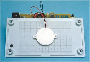
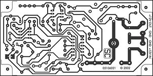
All the parts for the Battery Guardian are mounted on a single PC board, so it's a snack to build. This board is coded 05106021 and measures just 122 x 60mm. The completed assembly then fits neatly inside a standard plastic case measuring 130 x 67 x 44mm (see photo).
Start by inspecting the PC board for shorted tracks or breaks in the copper by comparing it with the published pattern. While you're at it, check that the holes are large enough for the component leads, particularly for the screw terminals.
Note also that the corners of the PC board must be shaped as shown on the PC layout diagram (Fig.2), so that it can be fitted into the box - ie, the corners have to be removed to clear the integral mounting pillars. You can remove the corners by first cutting out a rectangular piece using a small hacksaw and then carefully filing to shape using a round file.
Alternatively, you can use a mini-drill fitted with a small grinding disk (eg, a Dremel tool, or similar).
Fig.2 shows how the parts are fitted to the PC board. Begin by installing the three wire links plus two PC stakes to terminate the wiring from the piezo transducer. This done, install the resistors in the positions shown.
Table 1 shows the resistor colour codes but we recommend that you also check each value using a digital multimeter as some of the colours can be difficult to decipher.
Diodes D1 & D2 can go in next, followed by zener diodes ZD1 and ZD1. Take care to ensure that these are all installed the right way around and don't get ZD1 & ZD2 mixed up (their voltages are different).
Now for the three ICs. These are all soldered directly to the PC board, again making sure that they are oriented correctly. It's easy to identify pin 1 on each IC - it will be adjacent to a notch or dot at one end of the body.
Next, install the capacitors, taking care to ensure that the electrolytics are oriented as shown. That done, the transistors can go in but don't get Q2 and Q3 mixed up - Q2 must be a BC640, while Q3 is the BC327.
The Mosfet transistor (Q1) is mounted horizontally on a small heatsink and is secured using a 10mm M3 screw and nut. This means that you have to bend Q1's leads down by 90° before installing it on the board.
This is best done by first slipping an M3 screw through the device tab, positioning it on the board and then gripping one of the leads with a pair of needle-nose pliers just before it reaches its mounting hole. The device is then lifted clear of the board, the lead bent at right-angles and the procedure then repeated for the remaining two leads.
Once all the leads have been bent, the device can be secured to the PC board with its heatsink and the leads soldered. Note that it's not necessary to isolate the tab from the heatsink, since the heatsink doesn't touch any other parts. However, because Q1's tab is connected to its drain terminal (which is connected to the +12V rail), this means that the heatsink will be at +12V when the circuit is operating.
The PC board assembly can now be completed (except for transformer T1) by installing the 4-way screw terminal block, the fuse clips (make sure these go in with the retaining flanges towards the outside), pots VR1 & VR2 and the LED. The latter should be mounted so that the top of its plastic body is 30mm above the PC board.
By the way, we've provided two sets of mounting holes for the righthand fuse clip, so that you can use either a 3AG fuse or the shorter M205 type (the position shown on Fig.2 is for a 3AG fuse). Unless you have a good reason to do otherwise, stick with a 3AG fuse as these are more commonly available from service stations (note: M205 fuse clips are smaller).
We've also designed the board to accept the two commonly available trimpot sizes for VR1 and VR2. It's up to you which type you use.
Winding the transformer
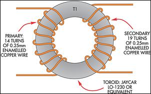
The primary and secondary of transformer T1 are wound on a ferrite toroid as shown in Fig.3. Wind on 14 turns of 0.25mm enamelled copper wire for the primary, in the direction shown. Similarly, wind on 19 turns for the secondary, in the direction shown.
Once the coils have been wound, scrape away the enamel from the ends of the leads and install the unit on the PC board. Make sure that you get the windings the right way around, with the primary towards IC1 and the secondary towards Q1. The toroid is then secured using short lengths of tinned copper wire which loop over either side of the core and solder to the PC board (see Fig.2).
Final assembly
There's not much to the final assembly, apart from drilling a few holes in the case and clipping the PC board into position.
The first step is to affix the front panel label to the lid. The label can then be used as a template for drilling the mounting holes for the LED (3mm) and the piezo transducer (2.5mm). You will also have to drill a small hole in front of the piezo transducer to let the sound out.
You also have to drill four holes in one end of the case, in line with the screw terminal block. This is best done by clipping the board into the integral slots in the case, marking out the hole positions, then removing the board and drilling the four holes to accept the power cables.
Once all the holes have been drilled, clip the board back into the case and mount the piezo transducer on the lid using two M2.5 x 10mm screws. The transducer's leads can then be soldered to the two PC stakes on the PC board.
Finally, install the fuse and you're ready for the smoke test.
Testing
Before applying power, check the assembly carefully to make sure that all parts are installed correctly. That done, apply power from the battery and use your multimeter to check for +12V on pin 8 of IC1, pin 8 of IC2 and pin 14 of IC3.
Assuming these are correct, check the voltage between Q1's gate and the "+12V IN+" terminal (positive lead to Q1's gate). You should get a reading of either 15V or 0V, depending on VR1's setting. If you get a reading of 0V, rotate VR1 anticlockwise until the reading jumps to 15V.
If the voltage only reaches a volt or two when you rotate VR1, check that you have wound T1 correctly. If you wind one of the windings in the wrong direction, the windings will operate in anti-phase.
Now adjust VR1 clockwise until you get a reading of 0V. LED1 should now flash once every 10 seconds or so and the piezo transducer should chirp when the LED flashes. Adjust VR2 for the best sound from the transducer.
Setting the cut-out voltage
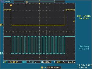
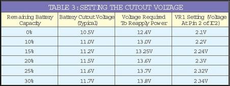
Table 3 shows how to set VR1 for various cut-out voltages from 10.5V to 11.7V. It also indicates the remaining battery capacity for each of these voltages but note that these are typical figures only and are not precise.
Basically, it's just a matter of selecting the desired cut-out voltage and adjusting VR1 to get the correct reading on the wiper. So, if you want to set the cut-out voltage to 11.5V, for example, adjust VR1 for 2.3V on its wiper (ie, 2.3V between the wiper and ground).
Generally, a cut-out voltage of about 11.5V or 11.6V is the way to go, since this leaves about 20% battery capacity in reserve for starting the car's engine. However, you can set the cut-out voltage higher or lower than this to suit your own particular requirements.
Installation

Be sure to use automotive power cable for all supply connections to and from the Battery Guardian.
Do not connect the Battery Guardian directly to the battery. If you don't wish to use the cigarette light socket, the +12V supply should be taken from a fused (but unswitched) terminal on the fusebox.
Note that if you wish to use the Battery Guardian with a large car stereo system, you cannot power all the amplifiers via the circuit because they are likely to draw more than 10A, which would exceed the fuse rating. Instead, the Battery Guardian would be connected in line with the supply to the head-end unit; ie, the CD/tape/tuner unit. That way, if the battery drops below the threshold, the head-end unit will be cut off and so the current drain from the amplifiers in the system will drop to a low value.
Finally, the Battery Guardian could also be used to protect the batteries in a 12V lighting system, with the overall current limit again set by the 10A fuse.
| Parts List
1 PC board, code 05105021, 122 x 60mm |
| Table 1: Resistor
Colour Codes
|
| Table 2: Capacitor
Codes
|
| The following downloads are available for this article: |